Making electronics projects and finally watching them work is very interesting. But assembling components on a general purpose PCB is very cumbersome. It’s is a very time consuming task and sometimes the circuit mess up so much that it becomes irritating to work. It will be a great if one can fabricate PCB (Printed Circuit Board) for electronics projects at home. It is an interesting task for any electronics hobbyist. It saves time to complete a project and also increases the reliability of project. Getting PCB fabricated from market is a costly affair, also the fabricators demands the PCB quantity to be large. For any hobbyist it is easy to fabricate PCB at home using material easily available at home. A widely used method for making PCB is the TONER TRANSFER method used by most of the electronics hobbyist.
Material required:
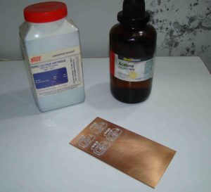
- Copper clad
- Laser printer
- Photo Paper/Magazine glossy paper
- Iron
- Rubber gloves
- Ferric chloride
- Plastic tray
- Acetone/Nail paint remover
- Scrubber or steel wool
Cleaning
First of all clean the PCB clad using the scrubber to remove any oil and dust stains from the surface of the clad. After cleaning the clad surface make it dry. Avoid touching the surface of the clad after drying.

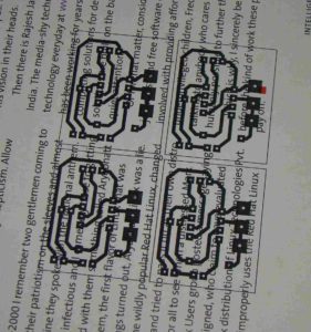
Printing Layout
Print the layout on glossy side of the photo paper using the laser printer. Keep the ink density at maximum level (print at maximum resolution). The layout should be printed mirrored on glossy paper without any scaling (use 1:1 print). Photo-paper and projector transparencies can also be used
Transferring Layout
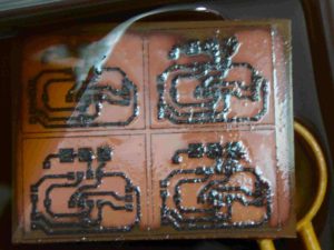
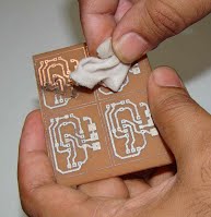
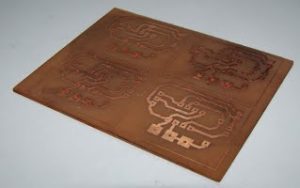
Transferring layout form photo paper to the copper clad requires a little experience. Place the printed paper on copper clad and press it with hot iron. Use irons nose to apply pressure on edges of the copper clad. After a while when the color of paper turns yellowish try peeling the paper from clad. Check the clad for proper transfer of layout pattern. If first attempt is not a success, repeat the same procedure to get the layout transferred successfully. You can use black permanent maker to fix the missing tracks Once the pattern is transferred successfully on copper clad the next process is removal of unwanted copper.
![]()
![]()
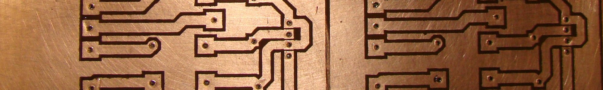
Etching
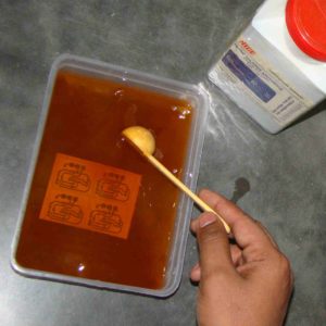
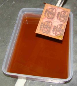
To remove unwanted copper from clad ferric chloride is commonly used as an etching solution. Ferric chloride is easily available on chemical stores. Make a solution of ferric chloride with warm water in a plastic tray. Quantity of ferric chloride depends on size of PCB to be etched. Generally two tea spoons are enough for medium size PCB. Dip the PCB inside the ferric chloride solution. Keep stirring the solution to accelerate the etching process. After a few minutes you will see copper vanishing from the edges of the clad. Wait until the etching process completes. Use rubber gloves and safety glasses while dealing with ferric chloride. Avoid contact with body parts and eyes.When all exposed copper is etched completely take out PCB from solution and wash it with water.